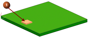
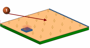
Thermal analysis of a PCB with a chip
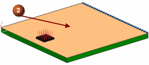
In this tutorial, you will simulate the heat transfer from an electronic chip to the printed circuit board (PCB). This tutorial presents Simcenter 3D Thermal.
-
On your desktop or the appropriate network drive, create a folder named pcb-w-chip.
-
Click the link below:
-
Extract the part files to your pcb-w-chip folder.
-
Start Simcenter 3D or NX.
|
File |
-
 Open (Standard toolbar)
-
Files of type
Part Files (*.prt)

-
File name
pcb-w-chip.prt
-
OK
The options you select in dialog boxes are preserved for the next time you open the same dialog box within a given session. Restore the default settings to ensure that the dialog boxes are in the expected initial state for each step of the activity.
|
File |
Preferences→User Interface
-
Options
-
 Reset Dialog Memory
 -
OK
|
Application |
-
 Pre/Post (Simulation group)
![]() Simulation Navigator
Simulation Navigator
-
 pcb-w-chip.prt
 -
 New FEM and Simulation
 -
Solver
Simcenter 3D Thermal/Flow
-
Analysis Type
Thermal
-
OK
-
Name
PCB_chip_solution
-
OK
Solution dialog box
![]() Simulation Navigator
Simulation Navigator
-
pcb-w-chip_fem1.fem
-
Make Displayed Part
Start by creating an orthotropic material you will use for the PCB.
A value of 1 is used for non-thermal properties as these are required by the interface
but not used during the analysis.
The material density is 2700 kg/m3, the specific heat is 396 J/kg·K, and the orthotropic thermal conductivities are 0.009 W/mm °C, 0.041 W/mm °C, and 0.00055 W/mm °C in the X, Y and Z directions, respectively.
 Manage Materials (Home tab→Properties group)
-
New Material
-
Type
Orthotropic
-
 Create material
 -
Name
PCB_ortho
-
Note:
Verify the units of each property. To modify the units use the list beside the entry box.
Mass Density (RHO)
2700 kg/m3
-
Thermal/Electrical
-
Specific Heat (CP)
396 J/(kg·K)
-
Thermal Conductivity
-
Thermal Conductivity (K)
0.009 W/(mm·°C)
-
Thermal Conductivity (K2)
0.041 W/(mm·°C)
-
Thermal Conductivity (K3)
0.00055 W/(mm·°C)
-
OK
Orthotropic Material dialog box
-
Close
Manage Materials dialog box
This is a simplified example. NX PCB Exchange and Simcenter 3D Electronic Systems Cooling let you create complex orthotropic board conductivities with information imported from ECAD files.
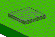
Create a 2D mesh for the PCB with an element size of 7 mm, and apply the orthotropic material you just created. The thickness of the board is 1.8 mm.
 2D Mesh (Mesh group)
-

-
Type
QUAD4 Thin Shell
-
Mesh Parameters
-
Element Size
7 mm
-
Destination Collector
-
 New Collector
 -
Type
Thin Shell
-
Material
PCB_ortho
-
Material Orientation
-
Material Orientation Method
Coordinate System
-
Material Orientation Type
Absolute
Note:The coordinate system you select defines the orientation of the orthotropic material properties. See the Pre/Post Help for more information.
-
 Create Physical (Thin Shell Property)
-
Name
PCB_thickness
-
Thickness
1.8 mm
-
OK
Thin Shell dialog box
-
Radiation
None
-
Name
PCB
-
OK
both dialog boxes
![]() Simulation Navigator
Simulation Navigator
-
 2D Collectors→PCB
 -
2d_mesh(1)
-
Rename
-
Change the name to PCB_mesh.
-
Enter
-
Esc
To model the chip, use a 3D tetrahedral mesh and apply an isotropic material with the following values: density 2700 kg/m3, thermal conductivity 383 W/m·K, and specific heat 380 J/kg·K.
 3D Tetrahedral Mesh (Mesh group)
-
-
Type
TET4
-
Element Size
5 mm
-
Destination Collector
-
New Collector
-
 Choose Material
 -
New Material
-
Type
Isotropic
-
Create material
-
Name
Chip_iso
-
Mass Density (RHO)
2700 kg/m3
-
Thermal
-
Thermal Conductivity (K)
383 W/(m·K)
-
Specific Heat (CP)
380 J/(kg·K)
-
OK
Isotropic Material dialog box
-
OK
Material List dialog box
-
Thermo-Optical Properties
-
 Radiation
 -
Name
Chip
-
OK
both dialog boxes
Change the name from 3d_mesh(1) to Chip_mesh.
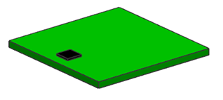
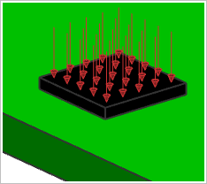
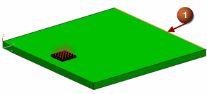
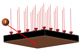
A heat load defines the power or energy per time applied into the selected geometry. Apply a 5 W heat load to the top surface of the chip.
![]() Simulation Navigator
Simulation Navigator
-
pcb-w-chip_fem1.fem
-
Display Simulation→pcb-w-chip_sim1.sim
-
pcb-w-chip_fem1.fem
-
 2D Collectors (hide)
-
3D Collectors (hide)
Only the polygon geometry is now visible.
 Thermal Loads (Loads and Conditions group→
 Load Type list)
-
Type
Heat Load
-
-
Name
Name
Heat_Load_5W
-
Magnitude
-
Heat Load
5 W
-
OK
The thermal load is applied to the chip.
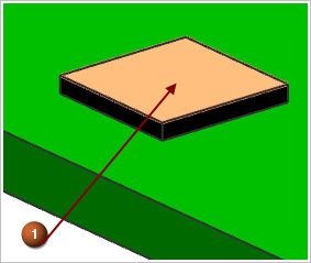
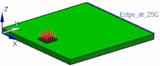
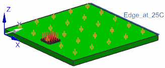
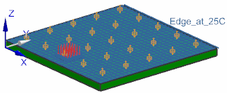
A temperature constraint defines known temperatures of a heat source or heat sink within the thermal model. Apply a temperature constraint of 25°C on the edge of the PCB opposite the edge closest to the chip.
 Temperature (Loads and Conditions group→
 Constraint Type list)
-
Type Filter
Polygon Edge
-
-
Name
-
Name
Edge_at_25C
-
Temperature
25 °C
-
OK
The temperature is applied to the edge.
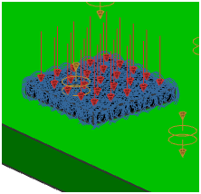
A thermal coupling models conduction between the entities of components that are physically or thermally in contact. Create a thermal coupling between the chip and the PCB.
 Thermal Coupling (Loads and Conditions group→
 Simulation Object Type list)
-
Name
-
Name
Chip_to_PCB
![]() Simulation Navigator
Simulation Navigator
-
Polygon Geometry
-
Polygon Body (1) (hide)
-
Primary Region
-
 Polygon Body (1) (show)
-
Secondary Region
-
 Secondary Region
 -

-
Assume that the chip is connected to the PCB with a Ball Grid Array (BGA) solder connection with a total area that is half of that of the chip.
Assume a Pb-Sn weld with a thermal conductivity of 80 W/m-°C and a gap of 1 mm. You can now calculate a heat transfer coefficient:
Heat Transfer Coefficient =
ksolder * Asolder / (lgap * Achip)
Heat Transfer Coefficient =
80·0.5/ 0.001·1 =40000 W/m2·°C -
Magnitude
-
Type
Heat Transfer Coefficient
-
Coefficient
40000 W/(m2·°C)
-
OK
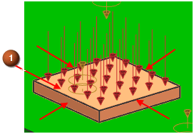
A convection constraint simulates convection for one or more surfaces by implicitly modeling the movement of fluid at a specific temperature in contact with one or more surfaces. Assume that the convection coefficient on the top and side faces is averaged to a single value of 24 W/m2°C.
 Convection to Environment (Loads and Conditions group→ Constraint Type list)
-
Name
-
Name
Chip_fan
-
(5 polygon faces)
-
Magnitude - Top
-
Type
Convection Coefficient
-
Convection Coefficient
24 W/(m2·°C)
-
Environment
-
Temperature
Specify
-
Temperature Value
30 °C
-
Apply
Do not leave the Convection to Environment dialog box.
Now create a convection to environment constraint for the PCB with a lower heat transfer coefficient of 19 W/m2°C from the PCB surface to air at ambient temperature of 25 °C.
-
Name
-
Name
PCB_convection
-
-
Magnitude - Top
-
Type
Convection Coefficient
-
Convection Coefficient
19 μW/(mm2·°C)
-
Environment
-
Temperature
Specify
-
Temperature Value
25 °C
-
OK
The run directory determines which directory is used to save the simulation files.
![]() Simulation Navigator
Simulation Navigator
-
PCB_chip_solution
-
Edit
-
Solution Details
-
Run Directory
Solution Name
-
Observe the other options available for Run Directory.
-
OK
Solution dialog box
![]() Simulation Navigator
Simulation Navigator
-
PCB_chip_solution
-
Solve
-
OK
-
Wait for Completed to display in the Analysis Job Monitor dialog box, before proceeding.
-
Yes
Review Results dialog box
-
Review the messages in the Solution Monitor dialog box.
-
 Solution Monitor dialog box
-
Information window
-
Cancel
Analysis Job Monitor dialog box
![]() Post Processing Navigator
Post Processing Navigator
-
Thermal
-
Load
-
Thermal
-
New Post View→Contour
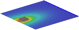
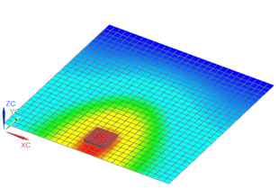
You can see the effects of the orthotropic material in the temperature distribution. Heat is better conducted in the Y direction. Temperatures vary from approximately 25 ºC to 60 ºC.
Observe the temperature variation on the chip and change the post processing display to banded. Each uniform band of color corresponds to the value limits shown on the color bar.
![]() Post Processing Navigator
Post Processing Navigator
-
Post View 1
-
 1D Elements (hide)
-
2D Elements (hide)
-
 Banded Display (Results tab→Display group)
-
 Feature (Display group→Edge Style list)
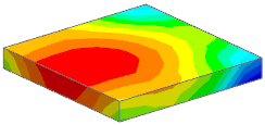
The post processing display updates. The average temperature is 60 ºC.
When you finish looking at the results, return to the model.
Save and close your files when you are finished.
|
File |
-
Save→Save All
|
File |
-
Close→All Parts